
The Window of Light: Why Silicon Photonics Is Becoming Strategic Infrastructure for AI and Quantum
From data‑centre optics to quantum sensing, silicon photonics is slowly becoming the backbone of national AI and semiconductor strategies, with the UK poised to become a global beachhead.

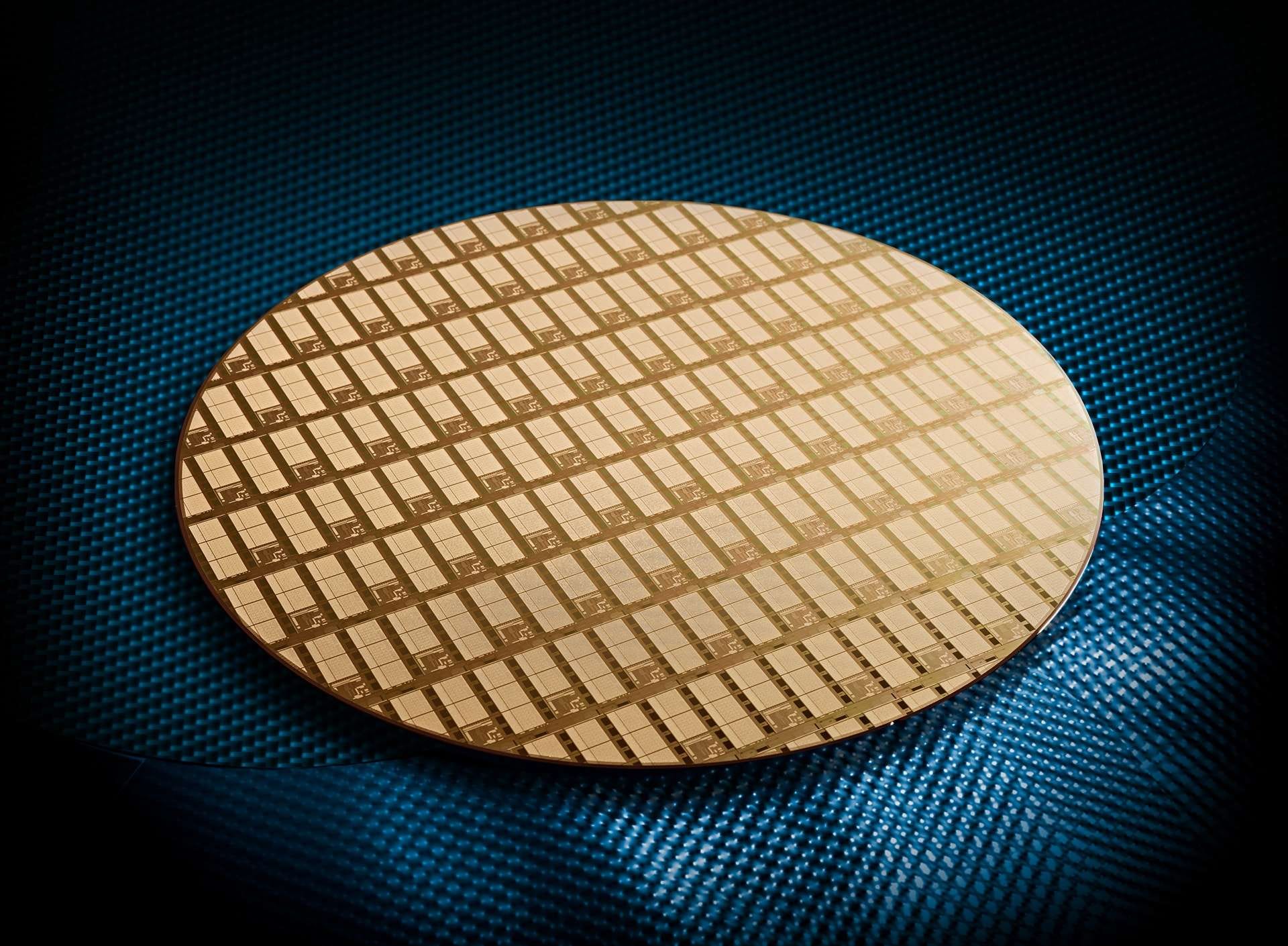
Silicon photonics now sits at the intersection of three powerful currents:
semiconductor manufacturing,
AI hardware, and
quantum sensing and communications.
In 2026, those currents are converging into a global infrastructure story about whether regions like the US, Europe, and the UK can build, own, and scale the fabs, pilot lines, and talent needed to turn thirty‑plus years of research into sovereign industrial capability.
At its core, silicon photonics is about putting light onto chips.
Photonic integrated circuits route photons through waveguides and optical devices fabricated on silicon, delivering far higher bandwidth at much lower energy per bit than traditional copper interconnects. This technology already underpins the fibre‑optic transceivers and co‑packaged optics that keep hyperscale data centres alive, quietly enabling the AI training runs and inference farms that have become part of the world’s critical infrastructure.
Globally, the data curve is a bit unforgiving:
“more parameters, more models, more sensors, more users, all demanding high‑speed, low‑latency connectivity between compute, storage, and the edge”
Traditional electronic links are hitting hard limits in power and performance. Silicon photonics offers a way out, turning light into a first‑class signalling medium on the same kinds of wafers and in the same kinds of fabs that already underpin the semiconductor industry. That makes it both a technological shift and an industrial one:
you don’t just need clever devices. you need
foundries,
prototyping lines, and
packaging ecosystems to make them at scale.
The US has already signaled the scale of its ambition.
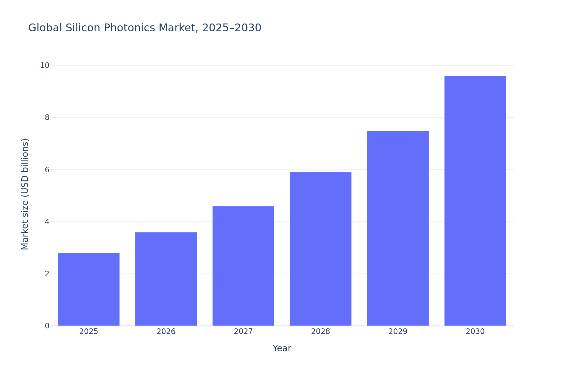
2026 market research report “Silicon Photonics: The Window of Opportunity is Open,” by CORNERSTONE sets out the global scale of the silicon photonics opportunity and the emerging race to capture it. It highlights major US federal and private commitments, including NVIDIA’s planned 6.5 billion dollar investment into silicon photonics, as part of a broader push to anchor AI infrastructure and data‑centre optics on home soil. the report contrasts this with European ambitions to build a flourishing SiPh industry through a 400 million euro photonic integrated circuit pilot line, and cites external market analysis projecting silicon photonics revenues of at least 46.5 billion dollars by 2035. Together with Asia’s existing manufacturing strength, this framing makes clear that we are not just watching a technology trend, but a global competition over who will own the infrastructure and sovereign capability underpinning the next generation of AI and quantum systems.
AI hardware enters the story as a tailwind rather than the sole destination.
Another highlight is the energy‑efficient optical AI accelerators and optical neuromorphic computing as emerging application, using light to perform the multiply‑accumulate operations and parallel data movement that define modern AI workloads.
interestingly, the same silicon photonics stack is also being pulled into 5G infrastructure, autonomous vehicle LiDAR, environmental sensing, and biomedical diagnostics, creating a broad base of demand that strengthens the case for investment in dedicated photonics infrastructure.
Quantum sensing and communications essentially add another layer of momentum to this.
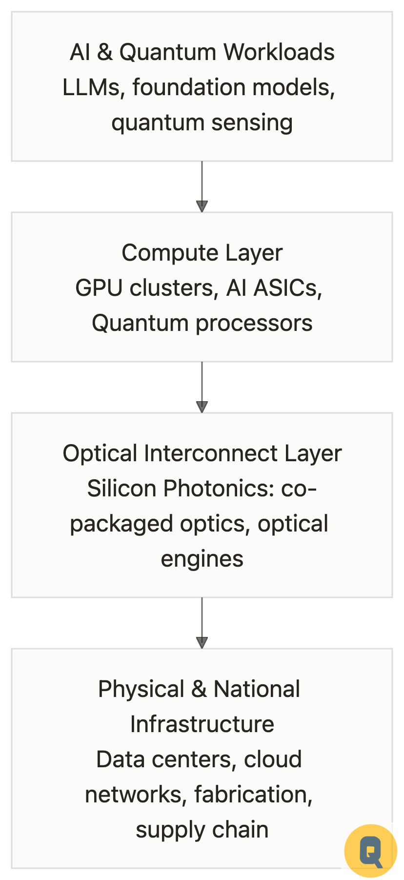
Silicon photonics offers a route to integrate sources, interferometers, filters, and detectors for quantum key distribution, quantum networking, and ultra‑sensitive measurement onto manufacturable platforms instead of bespoke optical benches. The report is explicit:
SiPh will “facilitate the scaling and practical application of quantum systems,” from communications to sensors, and this is one of the reasons the current window of opportunity is so time‑sensitive.
Regionally, this story is both optimistic and full of friction. The CORNERSTONE report surveys 500 decision‑makers across five markets - the US, UK, Germany, Spain and the Netherlands, and finds that confidence in the ability to scale silicon photonics is high everywhere, but highest in the US at 88 percent, followed by Spain at 87 percent and the UK at 82 percent, with Germany and the Netherlands slightly behind at 70 and 69 percent. That confidence is tempered by shared bottlenecks: prohibitive foundry costs, lengthy prototyping timelines, restrictive NDAs and licence terms (flagged by about a fifth of respondents), and high tariffs (cited as a major obstacle by roughly a third of respondents overall, with the UK figure matching that average).
This is what turns the narrative firmly into “semiconductor infrastructure” territory. that landmark growth depends on access to scale‑up infrastructure and commercial pilots as they bridge the gap between one‑off research runs and repeatable, qualifiable manufacturing that investors and customers can trust. Without them, promising designs stall at the prototype stage; with them, silicon photonics can ride the AI and quantum hardware waves instead of being swamped by them.
On the ground, the race is clearly multi‑regional. The US is signalling scale through multi‑billion‑dollar corporate bets and federal programmes, Europe is building shared pilot lines to seed a continent‑wide SiPh industry, and the report acknowledges Asia’s existing manufacturing strength as a key part of the global picture, and even though APAC was not part of this survey sample.
Against that backdrop, the UK’s distinctive play is to turn its research pipeline and open foundry model into a sovereign beachhead for silicon photonics, serving global customers while locking in local jobs, skills, and technological sovereignty.
In that sense, a silicon photonics and semiconductor infrastructure story, with strong AI hardware and quantum sensing/communications tailwinds isn’t just a tagline, it’s a comparative strategy, in which the chips that move our data and measure our environment are built on light, and the countries that control the photonic fabs and pilot lines effectively control key parts of the AI and quantum stack.
latest on the intelligent founder ai.

latest on the AI Unfiltered.

Copper is officially dead at the rack level. 🛑
When you force electrical signals through copper traces at terabit bandwidths, your power distribution network chokes instantly. Heat dissipation explodes. Resistance turns interconnects into thermal heaters. ⚡️
Silicon photonics isn't just a faster wire. It's a complete architectural reset for high-dimensional compute. Photonic integrated circuits route light through silicon waveguides, cutting energy per bit by orders of magnitude while eliminating trace cross-talk.
Here is the real bottleneck nobody talks about: thermal phase noise inside waveguides. 🧠
As wafer temperatures climb past 85°C, silicon's refractive index shifts dynamically. That phase drift destroys linear identifiability constraints in optical multiply-accumulate matrices. If you don't lock phase alignment directly at the physical gate, your optical matrix multiplication drops accuracy fast. 📉
We solve this by coupling optical switching matrices directly to SRAM-fused spectral phase-locking loops. By executing real-time phase compensation inside local L1 register tiles, we keep photonic vectors coherent without routing control signals through slow host software. Zero off-chip latency. Instant phase recovery. 🛡️
NVIDIA drop $6.5B into photonic infrastructure because they know HBM memory walls and copper heat limits will kill Next-Gen AI factories. Foundries and open pilot lines are the new geopolitical high ground. 🌐
Are your optical switches phase-locked at the silicon boundary, or is waveguide thermal noise silently corrupting your matrix multiplies? ⚡️
(•_•)